INCH�POUND
MIL�PRF�19500/586L
The documentation and process conversion measures
26 March 2014
necessary to comply with this document shall be
SUPERSEDING
completed by 22 September 2014.
MIL�PRF�19500/586K
22 April 2011
PERFORMANCE SPECIFICATION SHEET
SEMICONDUCTOR DEVICE, DIODE, SILICON, SCHOTTKY BARRIER,
TYPES 1N5817�1, 1N5817UR�1, 1N5819�1, 1N5819UR�1, 1N6761�1, AND 1N6761UR�1,
JAN, JANTX, JANTXV, JANS, JANHC, AND JANKC
This specification is approved for use by all Departments
and Agencies of the Department of Defense.
The requirements for acquiring the product described herein
shall consist of this specification sheet and MIL�PRF�19500.
1. SCOPE
1.1 Scope. This specification covers the performance requirements for silicon, Schottky barrier diodes. Four
levels of product assurance are provided for each encapsulated device types as specified in MIL�PRF�19500.
Two levels of product assurance are provided for unencapsulated devices (die) as specified in MIL�PRF�19500.
1.2 Physical dimensions. The device package styles are as follows: Axial leaded DO�204AL (formerly DO�41) in
accordance with figure 1 for device types 1N5817�1, 1N5819�1, and 1N6761�1, metal electrode leadless face
(MELF) DO�213AB in accordance with figure 2 for device types 1N5817UR�1, 1N5819UR�1, and 1N6761UR�1, and
unencapsulated die in accordance with figure 3 for device types JANHC and JANKC.
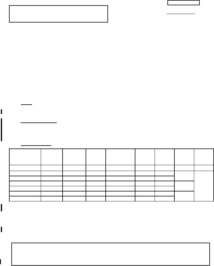
1.3 Maximum ratings. Unless otherwise specified, TA = +25�C.
IFSM
TJ
TSTG
VRWM
IO(PCB)
Max
Max
RΘJL
Types
TA = 55�C
RθJA
RθJEC
L = .375 inch
(3)
(1)
(2)
(9.53 mm)
(2)
�C/W
�C/W
�C
�C
V (pk)
A dc
A dc
1N5817-1
20
1.0
25
70
220
�65 to
1N5817UR-1
20
1.0
25
40
220
+125
1N5819-1
45
1.0
25
70
220
�65 to
�65 to
+125
+150
1N5819UR-1
45
1.0
25
40
220
1N6761-1
100
1.0
25
70
220
�65 to
1N6761UR-1
100
1.0
25
40
220
+150
(1) See figures 4, 5, 6, 7, 8, and 9 for derating curves and for effects of VR on TJ. TA = +75�C for both axial leaded
and MELF (UR) on printed circuit board (PCB), PCB = FR4 - .0625 inch (1.59 mm) 1-layer 1-Oz Cu, horizontal,
in still air; pads for UR = .061 inch (1.55 mm) x .105 inch (2.67 mm); pads for axial leaded = .092 inch (2.34
mm) diameter, strip = .030 inch (0.76 mm) x 1 inch (25.4 mm) long, lead length L ≤ .187 inch (≤ 4.75 mm); RθJA
with a defined PCB thermal resistance condition included, is measured at IO = 1 A.
(3) The maximum TJ depends on the voltage applied.
Comments, suggestions, or questions on this document should be addressed to DLA Land and Maritime,
ATTN: VAC, P.O. Box 3990, Columbus, OH 43218-3990, or emailed to Semiconductor@dla.mil. Since
contact information can change, you may want to verify the currency of this address information using the
ASSIST Online database at https://assist.dla.mil.
AMSC N/A
FSC 5961
For Parts Inquires call Parts Hangar, Inc (727) 493-0744
© Copyright 2015 Integrated Publishing, Inc.
A Service Disabled Veteran Owned Small Business